

Image Details
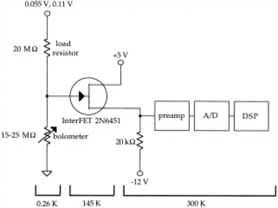
Caption: Fig. 9.
Bolometer electrical circuit. Shown is the signal path for a single detector. The bolometer forms a voltage divider with the 20 MΩ load resistor. For the bolometers in the top of the array (higher G), the bias voltage is 0.11 V. For the bolometers in the bottom of the array (lower G), the bias voltage is 0.055 V. A JFET voltage follower located in a 145 K box inside the Dewar lowers the impedance of the bolometer signal. The AC‐coupled preamplifier stage is normally operated with a gain of 10,000, and the voltage is digitized with a 16 bit analog‐to‐digital (A/D) converter. The preamplifier box bolts onto the outside of the Dewar, and the A/D box is located nearby. The digitized signals are transmitted serially over a fiber‐optic cable to a digital signal processor in the data acquisition computer, located in the observatory control room. The A/D and digital signal processor hardware were designed at NASA Goddard Space Flight Center.
Other Images in This Article
Copyright and Terms & Conditions
© 1998. The American Astronomical Society. All rights reserved. Printed in U.S.A.

