Image Details
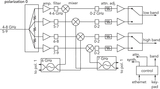
Caption: Figure 7.
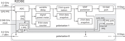
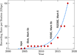
Functional diagram of the R2DBE. A pair of ADCs sample two channels of 2.048 GHz Nyquist bandwidth IF bands, typically representing two antenna polarizations. After requantization of the samples to 2 bits, the data are distributed in VDIF packets over a 10 GbE network to Mark 6 recorders. The maximum FPGA clock speed is too slow to process the ADC output stream rate of 4096 megasamples per second in series, so 16 ADC samples are transferred from the sampler in parallel on each FPGA clock cycle and are processed in parallel though the FPGA, which is clocked at a sixteenth of the sample clock, or 256 MHz. The FPGA and sampler clocks are locked to the maser reference frequency. In addition to the sample clock and dual IF inputs, each ADC circuit board is also equipped with a low-frequency synchronization input. On one of the ADC boards, the synchronization input is connected to GPS PPS. An internal PPS for VDIF time stamping is synthesized from the 2.048 GHz maser-referenced clock and synchronized to the GPS real-time PPS time-tick once at the beginning of an observation. The internal PPS drift relative to GPS real-time PPS (Figure 5) is measured by a counter and is available to be read from a register over Ethernet, as well as copied into the VDIF data-header, as it is a prior parameter for VLBI correlation.
Other Images in This Article
Show More
Copyright and Terms & Conditions
© 2019. The American Astronomical Society.