Image Details
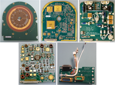
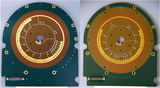
Caption: Figure 6.
All of the electronics boards that are part of the electronics package for a single SPAN-E. Top left panel: SPAN-Ae anode board without MCPs or MCP mounting structure attached. The hole in the center is for the HVPS signal to pass through the boards below and reach the hemisphere. Top center panel: SPAN-E Digital board, including FPGA and memory modules. The SPAN-E FPGA puts packets in CCSDS format for receipt by the SWEM. Top right panel: SPAN-E HVPS, which creates hemisphere, deflector, MCP bias, and spoiler voltages, which are sent either though the center holes in the digital and anode boards, or through the backplane (bottom right). Bottom left panel: SPAN-E LVPS, which generates 1.5, 3.3, 8, and 5 V for SPAN-E. Bottom right panel: backplane board for SPAN-E. The digital, HVPS, and LVPS are connected through the backplane. The connectors coming out of the top of the backplane supply signal to the attenuator and the high-voltage signals to the spoiler and deflectors. The enable plug is not installed in the image.
Other Images in This Article
Show More
Copyright and Terms & Conditions
© 2020. The Author(s). Published by the American Astronomical Society.